LMS6002D – The World’s First Field-Programmable RF Chip
First published in EE Times
Paul Dillien, Principal, High Tech Marketing
Today, my topic covers an entirely different type of programmable device, which is referred to as a field-programmable radio frequency (FPRF) chip. But first, let's start with a very quick look at the traditional field-programmable gate array (FPGA) concept.
As we know, FPGAs evolved from simple glue logic consolidation to being capable of implementing complex digital functions. Along the way, they have included a growing range of hard logic cores and functions such as processors and dedicated interface blocks. Some FPGAs also feature sophisticated analog functions such as high speed transceivers, but -- generally speaking -- FPGAs have really only touched the fringes of the analog world.
In contrast, the FPRF comes from the wireless domain and brings exciting new possibilities. At the highest level of abstraction, the FPRF transmitter takes a digital data stream and converts it into wireless signals, while the receiver perform the inverse operation. Add to this the capability to program key parameters like the RF frequency, gain, and bandwidth, and you have the essential ingredients of an FPRF chip as illustrated in the block diagram below:
When I first learned about the device, I could see that it brings similar capabilities for RF to those offered by FPGAs in the logic domain. Firstly, it is programmed by customers, not in the factory. Secondly, the tools allow customers to experiment and change parameters on the fly. Thirdly -- and most importantly -- the applications are limited only by the imagination of the user.
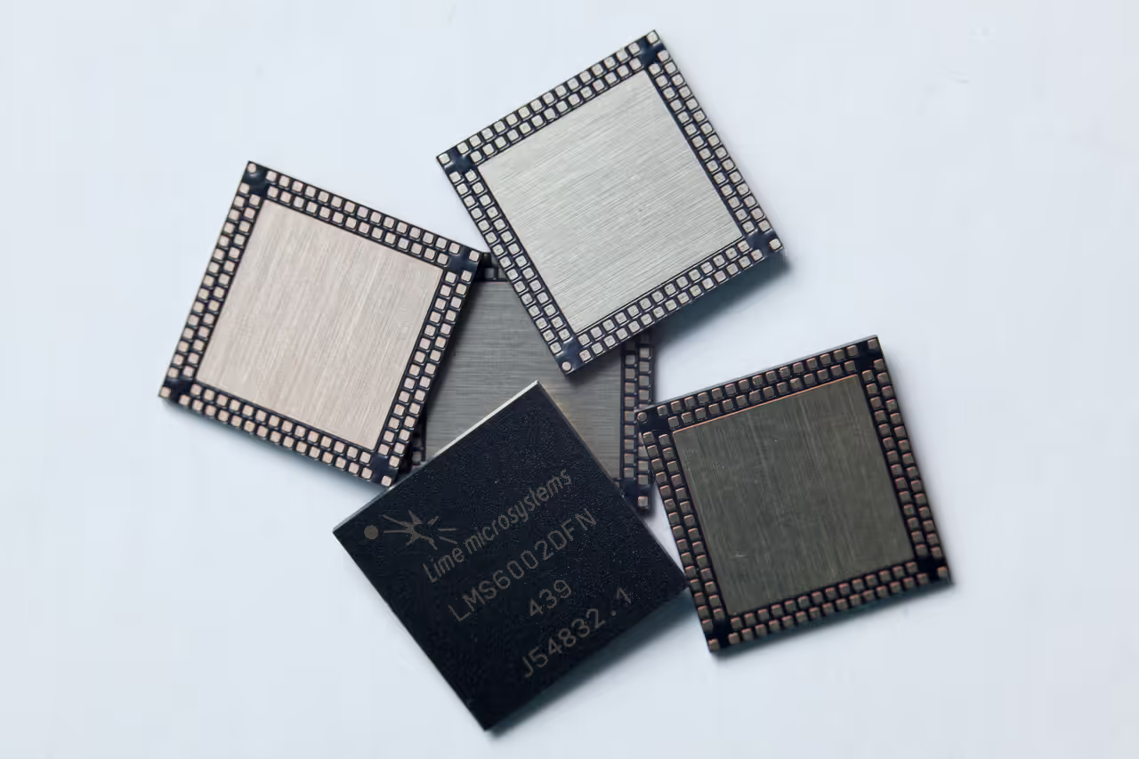
The FPRF chip is fabricated in the US for a UK company called Lime Microsystems. The part number is LMS6002D, but Lime coined the acronym FPRF because it captures the essence of the product.
So let's take a deeper dive into the product. Wireless transmission uses a range of different modulation schemes, and the chip accepts data as In-phase (I Data) and Quadrature (Q Data) words. The transmit path applies the data to a pair of on-chip DACs to convert it into two analog signals. The user can choose to bypass the DACs and inject analog signals directly into the device or monitor the DAC outputs.
The next operation involves filtering the signal. The pass band of this filter is programmed by the user to one of 16 different bandwidths ranging from 1.5 to 28MHz. The filtering restricts the signals to the selected bandwidth, and attenuates any out-of-band noise or aliasing from the DAC. The block diagram for the transmit (TX) path is illustrated in the following diagram:
The filter can boost the signal by 6dB, and is followed by a programmable baseband gain stage that can be adjusted to give up to 31dB of gain in 1dB increments. The signal is then mixed to directly give the required modulated RF frequency output. The TX PLL synthesizer multiplies up the input PLL clock by a programmable ratio, and generates a stable frequency with a tight accuracy. The RF gain stage (programmable, of course) provides the final signal boost that is output from the FPRF device. The transmit power level is sufficient for short range communications, say, tens of meters, without any further amplification. Users can use external amplification to increase the range.
Not surprisingly, the receiver path is also highly programmable. The FPRF device offers a choice of three low noise amplifiers (LNAs). A general broadband input stage is designed to handle RF inputs across the spectrum from 300 MHz to 3.8 GHz. Two further LNAs are optimized for enhanced performance for signals in the range 300 MHz to 2.8 GHz (Lo LNA) and 1.5 to 3.8 GHz (Hi LNA). The block diagram for the receive (RX) path is illustrated in the following diagram:
The mixer in the receive path uses the same PLL clock input as the transmitter, but has a different synthesiser to provide full duplex and direct down conversion. Programmable gain stages and filtering are applied, before the analog signal is digitised and output as I&Q data streams.
Configuration of all the different elements is performed via a simple SPI interface into the control logic. Each element is programmed by loading a 16-bit word that can be static or -- for more sophisticated applications -- the parameters can be changed on the fly (more on this later).
The configuration is set up using a simple GUI (graphical user interface) that allows control of the features described above, as well as test and loopback modes. This GUI is illustrated below:
Thus far we've considered a simplified description of the mechanics of the device -- but what can you use it for? Well, the chip was designed to be highly flexible, because one of the key applications is for cellular femto and pico cells, as I'll explain. These boxes act as local base stations for cell phones, and link into the internet to provide fast connectivity inside the home or small office. For example, the nearest tower to where I live is on the other side of a hill, so my reception is patchy at best. A femto cell would free me from reliance on signals from the tower.
The challenge in designing an RF chip for these applications is that cellular systems are different around the world -- with potentially over 40 different combinations needed on 4G or LTE phones to produce a truly global coverage. So the designers of the FPRF had to make it programmable so it wasn't restricted to a single market.
As soon as you have a chip that encompasses all the cellular frequencies, you also cover many other applications. For example, changing TV transmissions from analog to digital has freed up a bunch of spectrum for new wireless services. This is called "white space" and companies are working on a huge range of products as diverse as domestic appliances, smart metering, machine-to-machine (M2M) and rural broadband.
One application that Lime uses as a demonstration is a spectrum analyzer. The receiver in the chip is swept across the band to listen to all frequencies and the instantaneous output is displayed as the spectral plot. This demonstrates the ability of the FPRF chip to rapidly and dynamically change. Manufacturers of military systems were quick to grasp this, and are busily designing software defined radio (SDR) systems.
The spectrum analyzer uses a low-cost Myriad-RF evaluation board that is available to buy on an open-source website (sponsored by the company). Click here to find details of the board, data sheets, a user forum, downloads that include the FPRF configuration software, and a growing number of project ideas which will be added to the site over the coming months.
But the fun really begins when you combine an FPGA and an FPRF. All modern wireless systems owe a massive debt to digital processing to condition the signals and recover the data from amongst the noise. The Myriad-RF board can be connected to an Altera DE0-Nano board from TerAsic and to FPGA Mezzanine Card (FMC) Xilinx boards, including the whole Series-7 product range of Artix, Kintex, and Virtex All Programmable FPGAs and Zynq All Programmable SoCs. Appropriate Myriad-RF interface boards for the above can be ordered through Azio.
Access to both programmable RF and programmable logic opens up a world of new opportunities. For example, I've been looking into the possibilities for using FPRF devices in university teaching and research, which has uncovered a bewildering range of applications. Researchers are thinking about using the device for cellular applications where they can implement a particular algorithm in the logic domain and see the results in the RF output. Alternatively, the FPRF can receive weak signals, and researchers can try out different error correction schemes in the FPGA. Other possibilities involve using the chip for evaluating resource management algorithms for self-organizing networks, ground penetrating radar, or car-to-car communications.
The FPRF allows both professionals and hobbyists access to a flexible wireless transceiver, that will find its way into many new products over the coming years. Of course, it goes without saying that If you are planning to transmit wireless signals, don't forget to check your local regulations on permitted power levels and frequencies.
This article first appeared on All Programmable Planet, which was devoted to all things programmable.