LimeSDR USB
LimeSDR USB
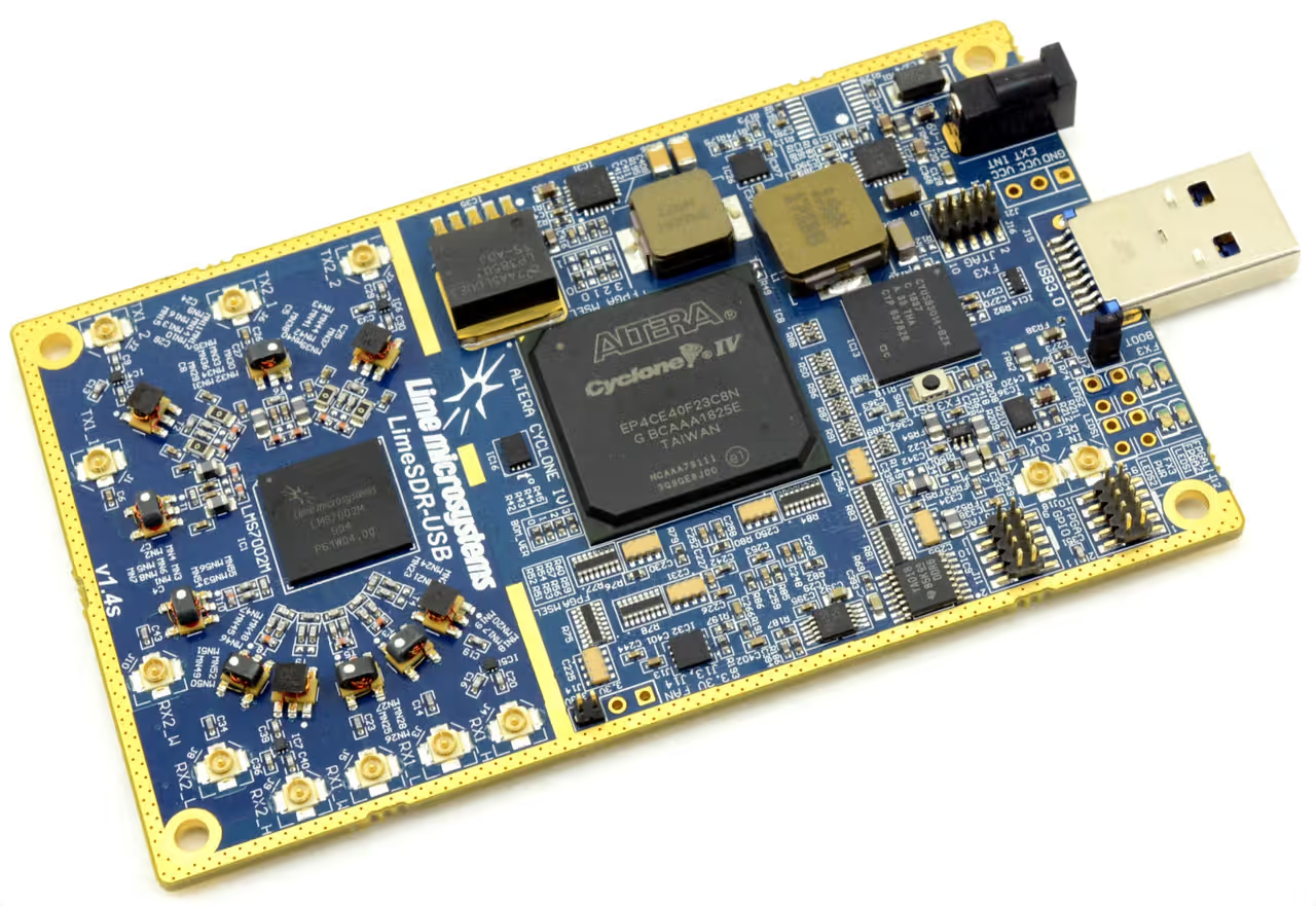
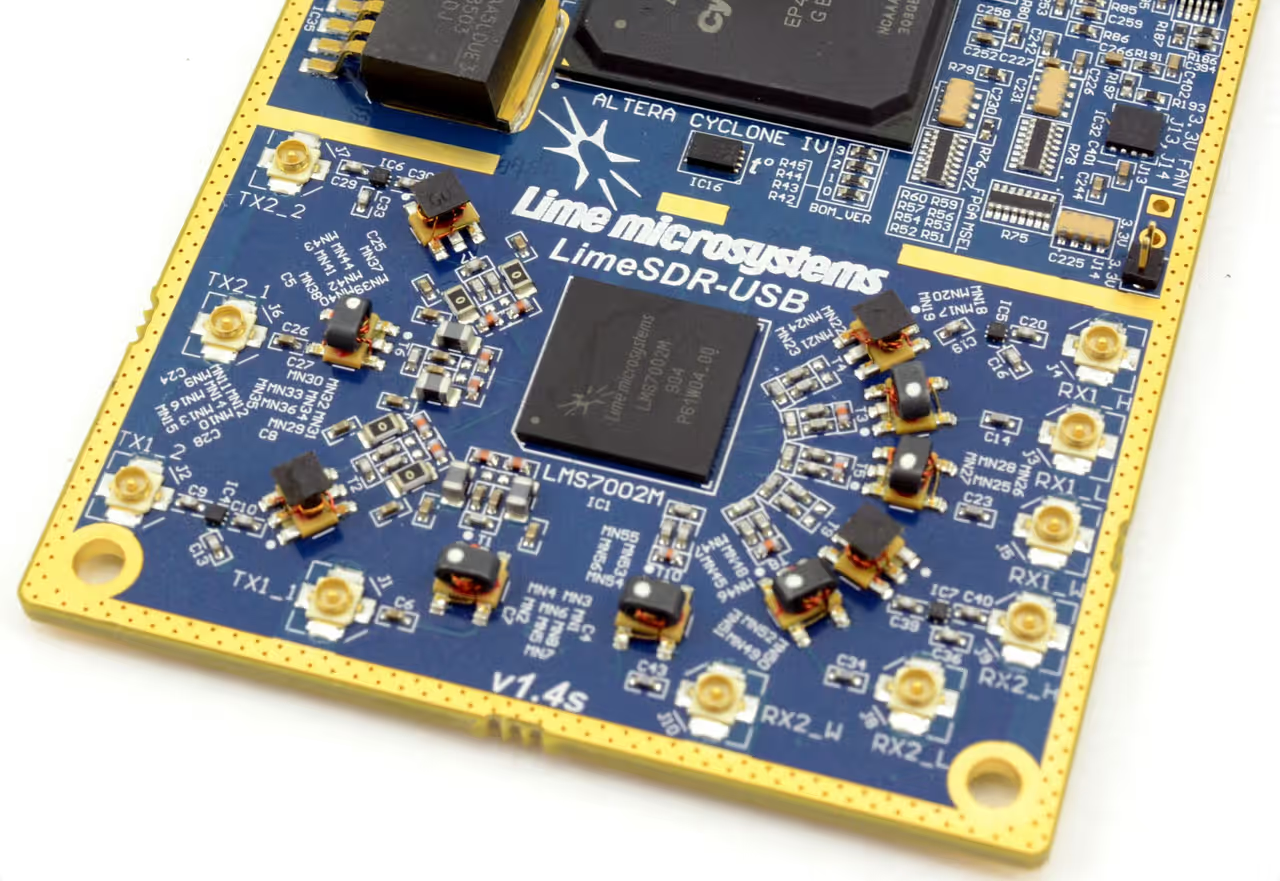
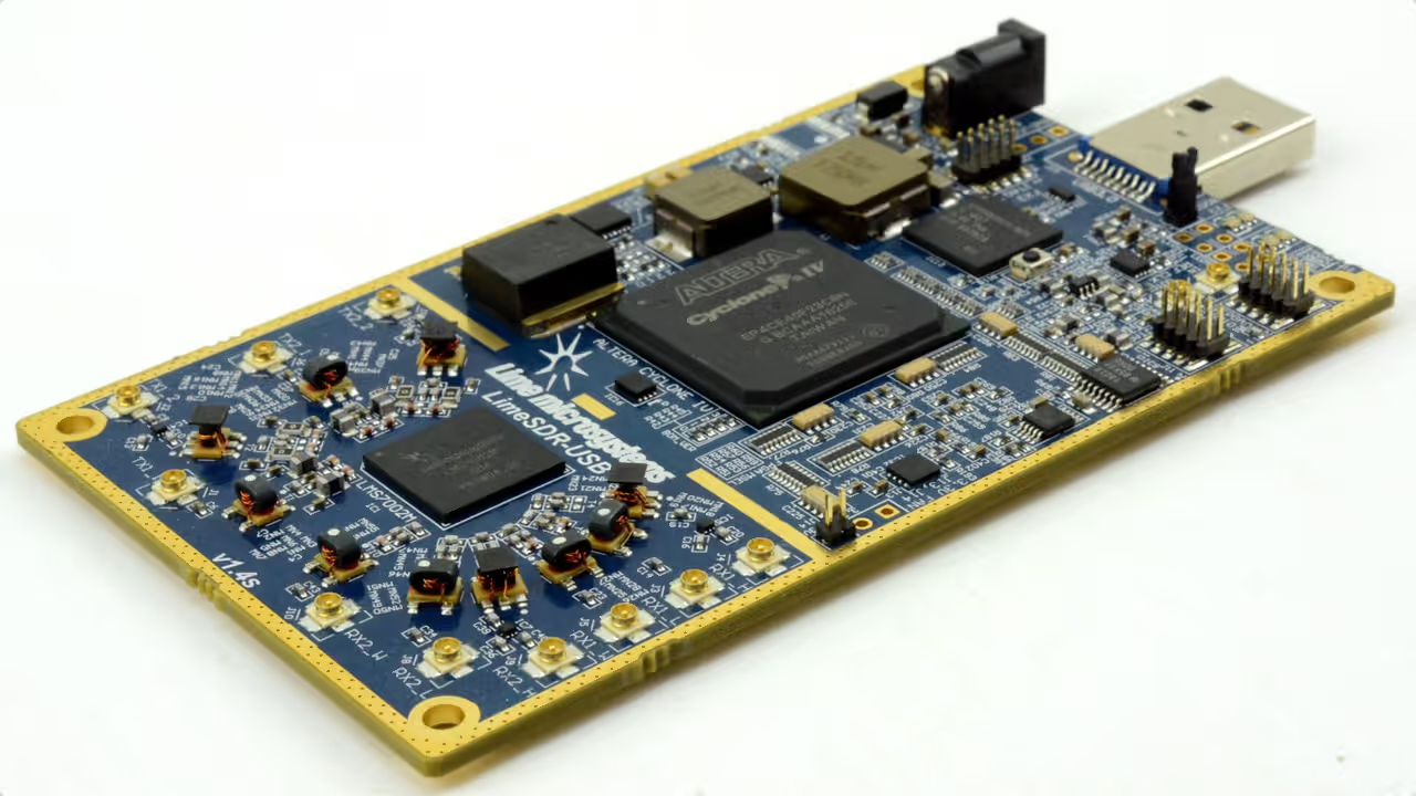
The original LimeSDR board drastically lowered the barrier for high performance 2x2 MIMO software-defined radio and it remains a popular choice with system builders, research labs and enthusiasts alike. Featuring Lime Microsystems LMS7002M RF transceiver at its core, together with an Altera Cyclone IV FPGA (40K LE) and Cypress FX3 USB 3.0 controller, LimeSDR USB provides a powerful platform for wireless innovation and other demanding RF applications.
The provision of 256 MBytes SDRAM memory means that in addition to streaming samples live via the USB 3.0 interface, waveform files can be loaded into memory and then “played” via one or both transmit ports. Thereby providing a unique and highly useful capability for lab use and specialist applications.
Setting the standard in flexible software-defined radio
LimeSDR USB has been employed in applications ranging from mobile networks, satellite communications and amateur radio, through to test equipment, education, spectrum monitoring and nuclear magnetic resonance (NMR), to name but a few. The sheer diversity of use cases and many thousands of boards sold are a testament to LimeSDR USB flexibility and ease of use.
Open-source PCB design, FPGA gateware, microcontroller firmware and host driver
The LimeSDRUSB PCB design and manufacturing databases are made available under a permissive open-source licence, along with the FPGA gateware, microcontroller firmware and host driver sources. Which means that anyone is free to take the hardware design and modify this for their own purposes, creating custom, application-specific and cost-optimised variants.
Lime has a longstanding commitment to open source and over 12 years ago founded MyriadRF, a family of open-source hardware and software projects for wireless communications, and a community that is working to make wireless innovation accessible to as many people as possible.
Specifications
- RF transceiver: Lime Microsystems LMS7002M
- Configuration: MIMO (2xTX, 2xRX)
- Frequency range: 100 kHz – 3.8 GHz
- Bandwidth: 61.44 MHz
- Sample depth: 12 bit
- Sample rate: 61.44 MSPS
- Transmit power: max 10 dBm (depending on frequency)
- FPGA: Altera Cyclone IV EP4CE40F23C8N
- 484-pin BGA
- 39,600 LUTs logic capacity
- 1,134Kbembedded Memory
- 116 x 18x18-bit multipliers
- 4 x PLL
- 532 x IO
- FPGA configuration via JTAG
- Cypress FX3 Super Speed USB 3rd generation controller
- 2x 1Gbit (64M x 16) DDR2 SDRAM
- 16 Mbit Flash memory for FPGA configuration
- 4Mbit flash for FX3 firmware
- 2 x 128K (16K x 8) EEPROMs for LMS MCU firmware, LMS MCU data
- 1 x 64K (8K x 8) EEPROM for FX3 data
- 30.72MHz onboard VCTCXO
- VCTCXO may be tuned by onboard DAC
- Programmable clock generator for the FPGA reference clock input or LMS PLLs
- Reference clock input and output connector (U.FL)
- 8 x GPIO (3.3V)
- USB3.0 (type A) plug
- Coaxial RF (U.FL female) connectors
- FPGA GPIO 10-pin header
- FPGA and FX3 JTAG connectors
- 6..12V DC power jack and pinheader
- Fan connector (3.3V)
- USB connector (5 VDC)
- DC barrel connector (6-12VDC)
- Dimensions: 60mm x 100mm